Presentation
Video
Make your own PCB Hacker Card
 maggie-j-liu
Reva went through this workshop & the components in a hat workshop and ended up making a custom pcb project for her club! For a bit of inspiration: check it out the slides.
This workshop will take about 60 minutes to design. After that, in a seperate 60 minute session you can order your board for manufacturing using the OnBoard grant tutorial.
Printed Circuit Boards - PCBs - are in nearly all electronics, from phones to cars! It's super easy to make your own, and make them not just functional, but also you can get creative with how they look.
In this jam, you'll design your own business card -- but with a twist -- it can transmit a URL on tap and light up! You'll learn the basics of designing a PCB, and you can get the cards made for free, with Hack Club's $100 OnBoard grant. With these skills, you'll be able to tackle even more complex boards, such as a custom macropad or fidget toy.
Schematic
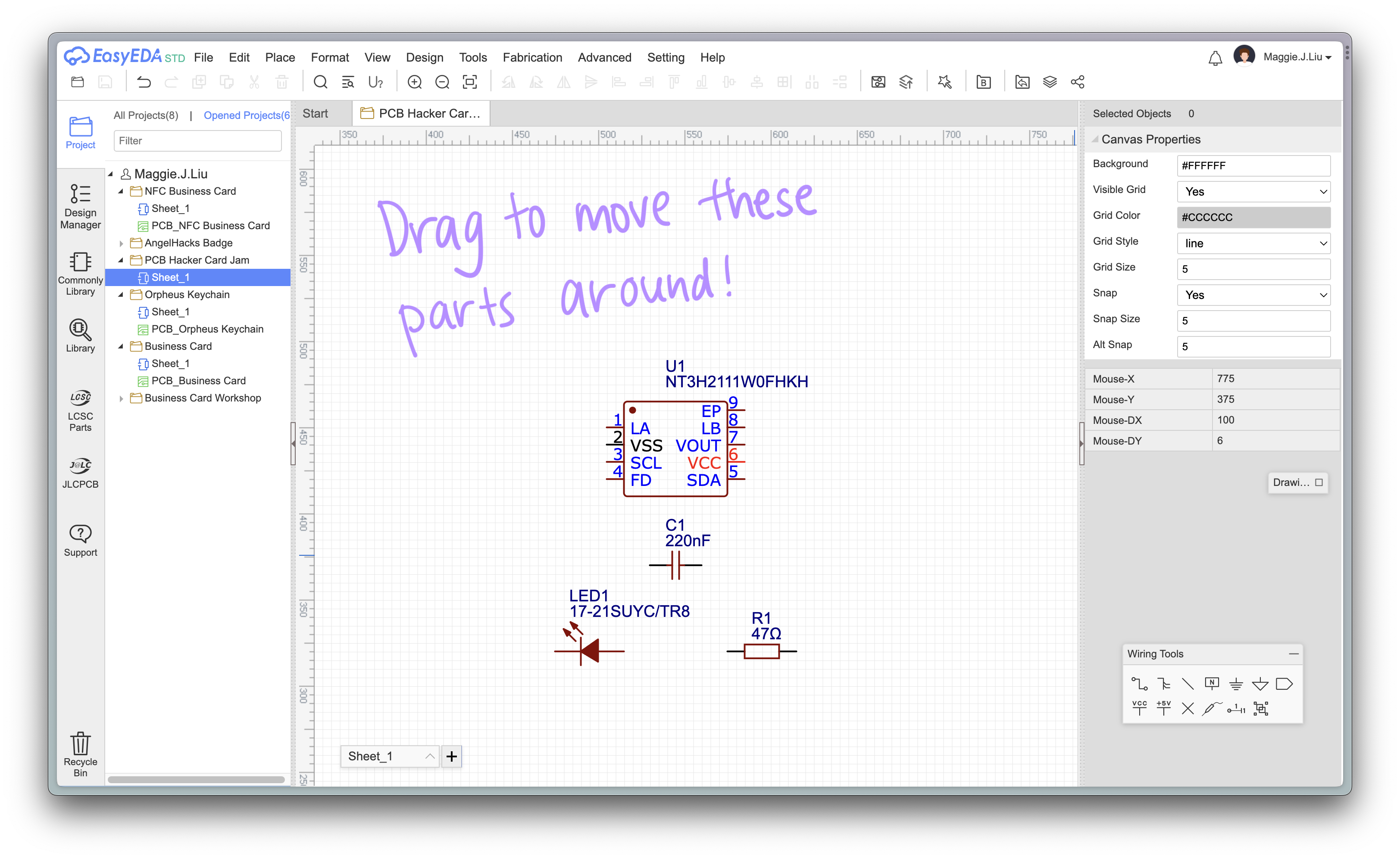
The first step is creating a schematic for your PCB design. A schematic shows the components that will be used in the circuit, as well as how each of these components connect to each other. An important thing to note -- a schematic is only a diagram of what connects to what, not where the components are actually placed on the board, so don't worry about placement at this stage!
First, let's open up EasyEDA, which is a browser-based (and free) PCB design tool. It can be a little bit tricky to get used to, so we made a very short video.
When you go to the website, you should see a screen like this. Click Sign Up to create an account, if you don't already have one.
Click on the EasyEDA Designer button in the Navbar to open up the schematic editor.
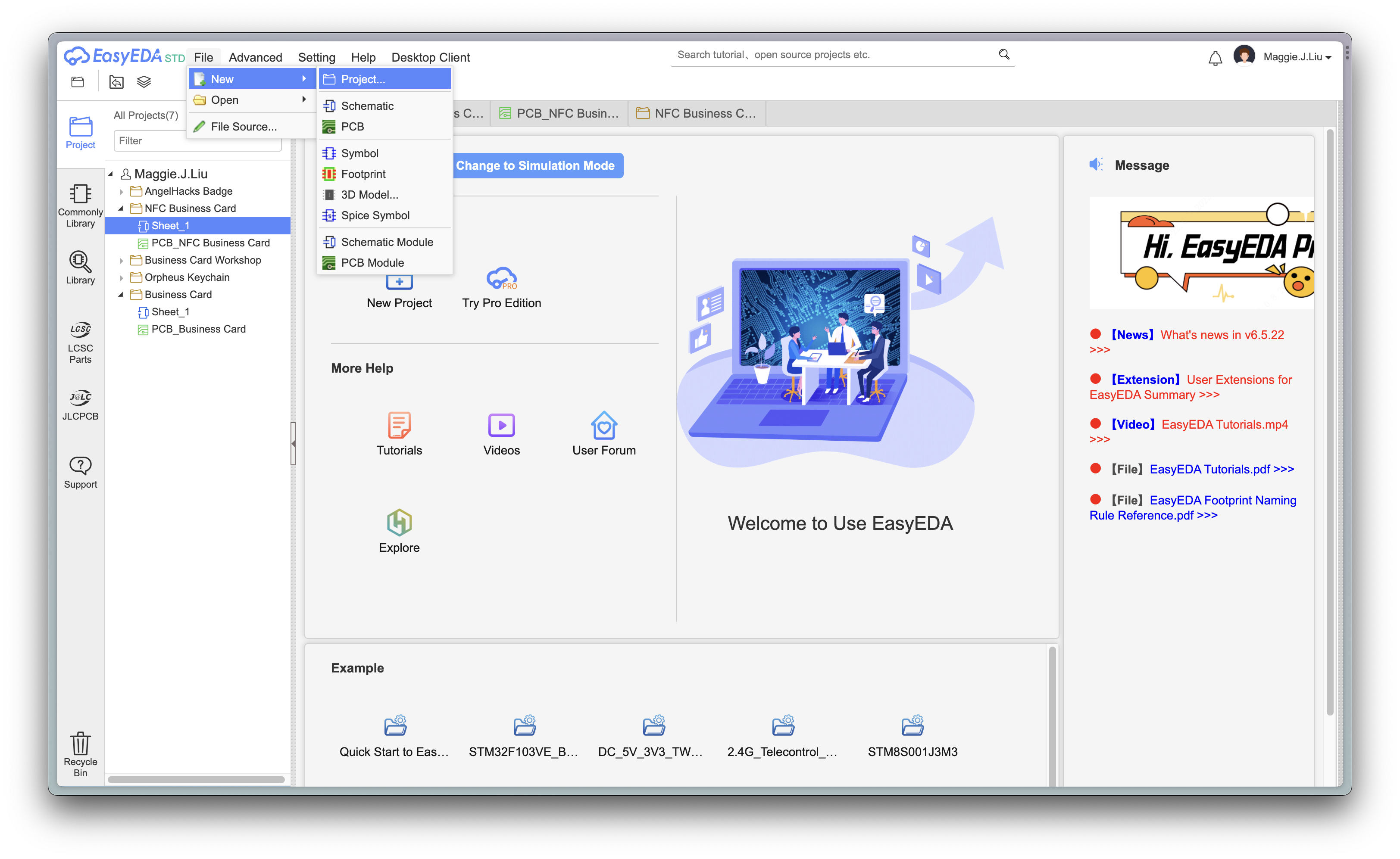
Once you've logged in, select File > New > Project to create a new project.
This will open up the schematic editor. Some important parts:
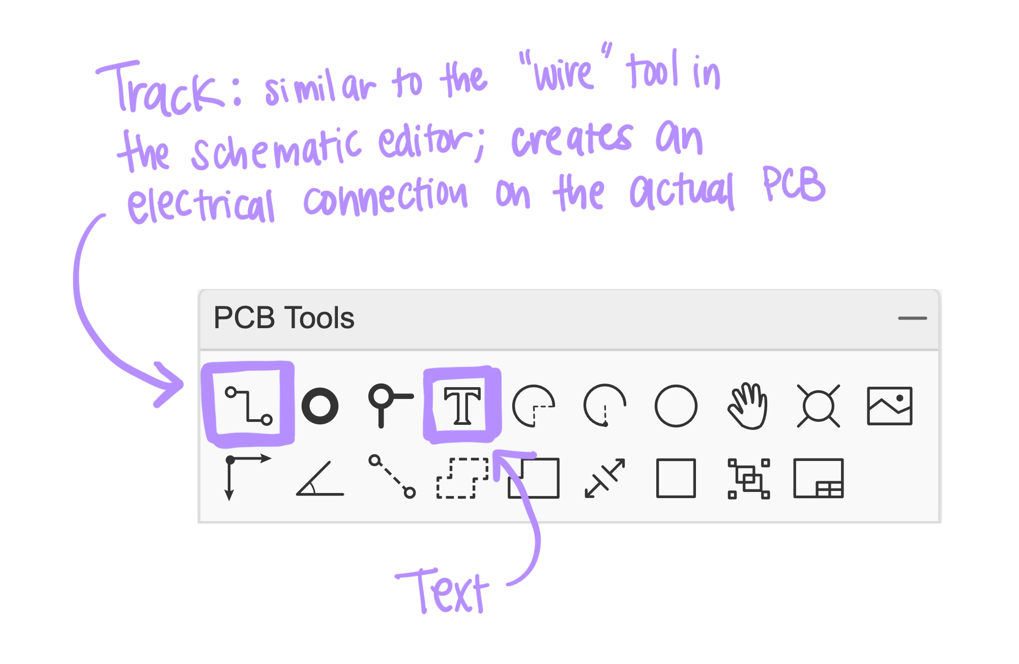
Libraryon the left toolbar: This is where we will search for components and place them into our schematic.Wiring Toolspanel: We'll be using the wire tool to connect the components together.
Placing components into the schematic
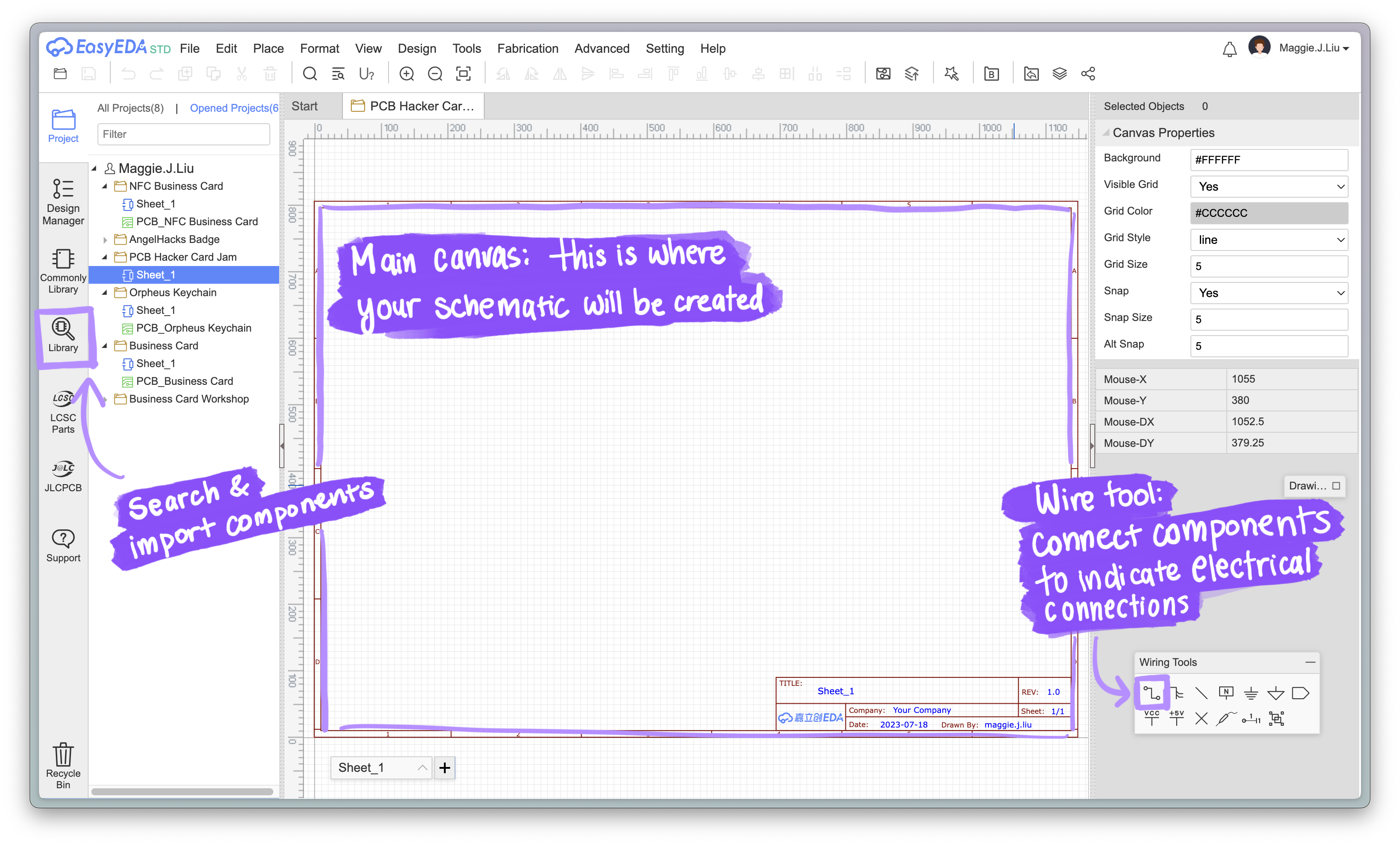
For our card, we'll want a capacitor, a resistor, a 2V LED and a NFC chip:
- A NT3H2111W0FHKH NFC Chip: this will be the main component of our card -- it both handles the NFC functionality as well as harvests energy from the phone to light up the LED
- An ~2V LED. I'm using C2296, but feel free to pick a different color (note: this part may also be called 17-21SUYC/TR8)
- A 47Ω resistor
- A 220nF capacitor
Click the Library button to open the parts picker. Search for a part (the part number works best), and make sure JLCPCB Assembled is selected. This will make sure we're choosing parts from JLCPCB's parts library, as this is currently Hack Club's Onboard PCB manufacturer.
Select the part, then hit the Place button to add it to your schematic. Repeat for all 4 of the parts listed above.
Note: The EasyEDA parts library may not always be helpful when finding parts for your own future projects, so feel free to search the internet for parts and their codes. You can also create your own parts, but that's a bit more advanced.
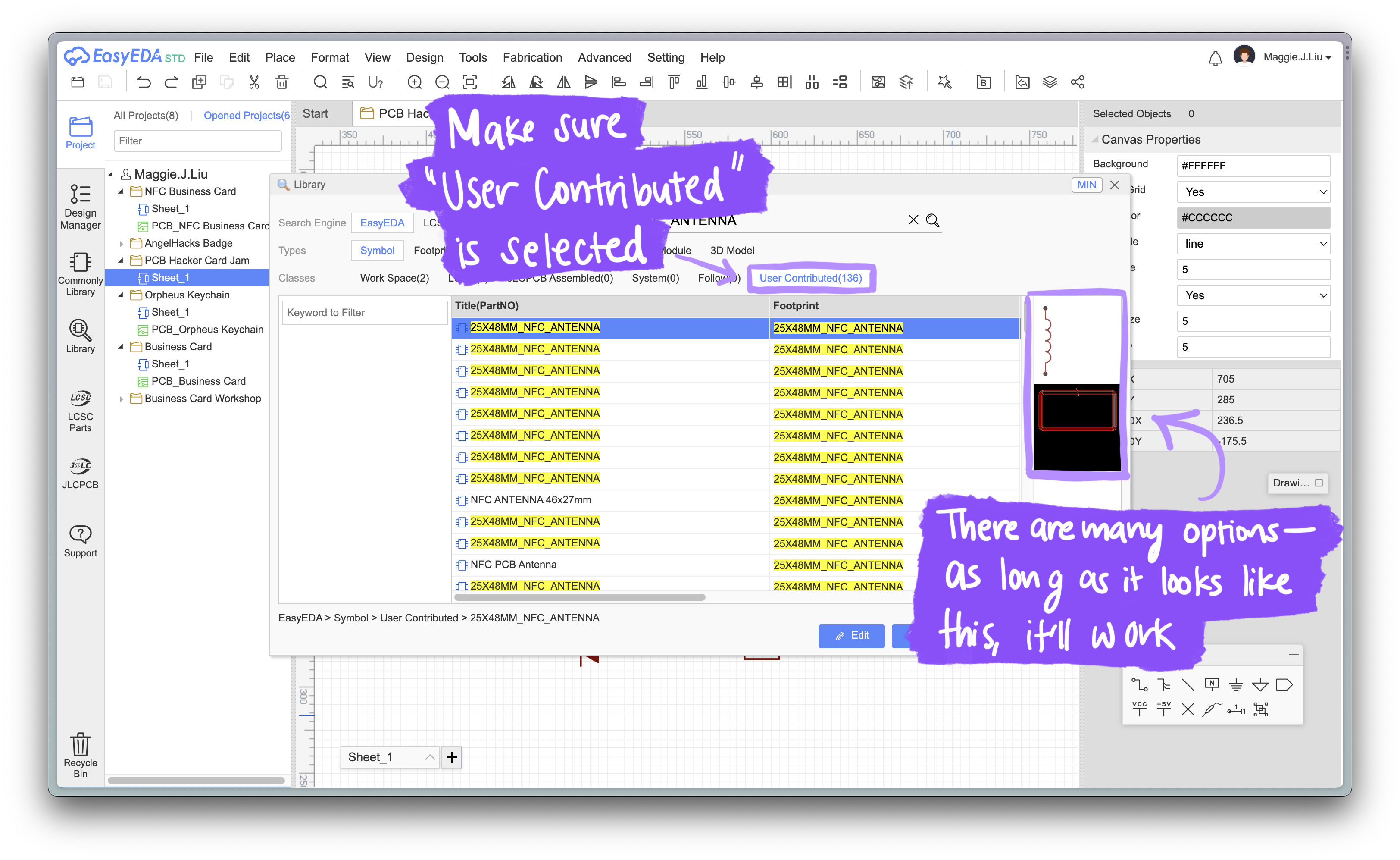
Adding the antenna
The NFC chip needs an antenna to work. We'll be using a PCB trace (a line of copper in the board) as the antenna, so we'll need to add that to our schematic.
Note: this is not an actual part, so it doesn't need to be assembled onto the board -- it's formed by the copper traces on the PCB.
To add the antenna, search for 25X48MM_NFC_ANTENNA in the Library, and instead of JLCPCB Assembled, select User Contributed. Select one of the options (check the preview to make sure it looks similar to the one I used here, but most of them should work), and place it on your schematic.
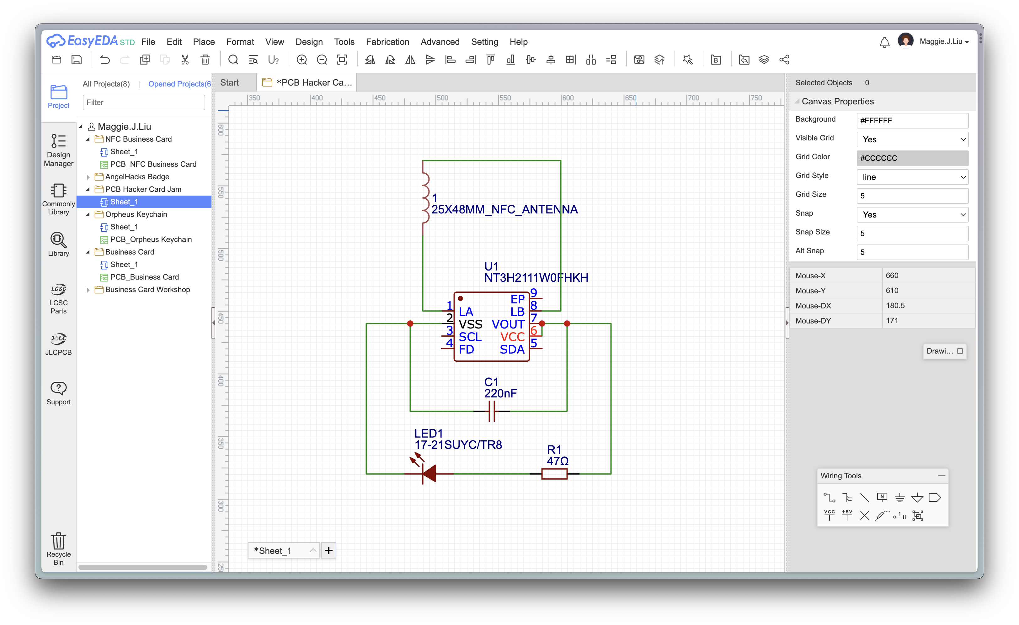
Wiring up the components
Now that all of our components are placed, let's connect them together! Make sure to save your work (command-s or control-s) as you go along.
The Wire tool indicates an electrical connection between the different parts -- this is similar to how you would connect wires on a breadboard. On the actual PCB, copper traces will go where we added wires, to form those electrical connections.
We'll reference the NFC Chip's Datasheet (yes, that obscure, horrifyingly detailed document), specifically this explanation for creating an energy harvesting circuit.
The datasheet says
A complete total connected capacitor in the range of typically 150 nF up to 220 nF maximum shall be connected between VOUT and GND
So we'll connect the capacitor between VOUT and GND (the VSS pin).
-
The pins
LAandLBare for the antenna, so we'll wire up the antenna between those two pins. -
If NTAG I2C also powers the I2C bus, then VCC must be connected to VOUT
Since the NFC chip will use the power transmitted from the phone to power the chip itself, we'll connect
VCCtoVOUT. -
Finally, to complete the circuit and light up the LED, we'll connect the LED and resistor between
VOUTand GND (theVSSpin).
Your schematic should look something like this when completed:
Note that your schematic may look a bit different from mine -- that's okay! As long as the connections are the same, it should work. So feel free to experiment with different layouts, maybe keep the antenna on the right or change the position of LEDs and resistors? It's up to you!
Friendly reminder to save (command + s or control + s) your work! You can also click Project > Save Project to save your schematic.
Designing the PCB
Now that the schematic is complete, we can start designing the actual PCB. In this step, we'll place the components onto the board, in the exact shape and configuration that the final board will be. The schematic is our guide to how to connect the components together.
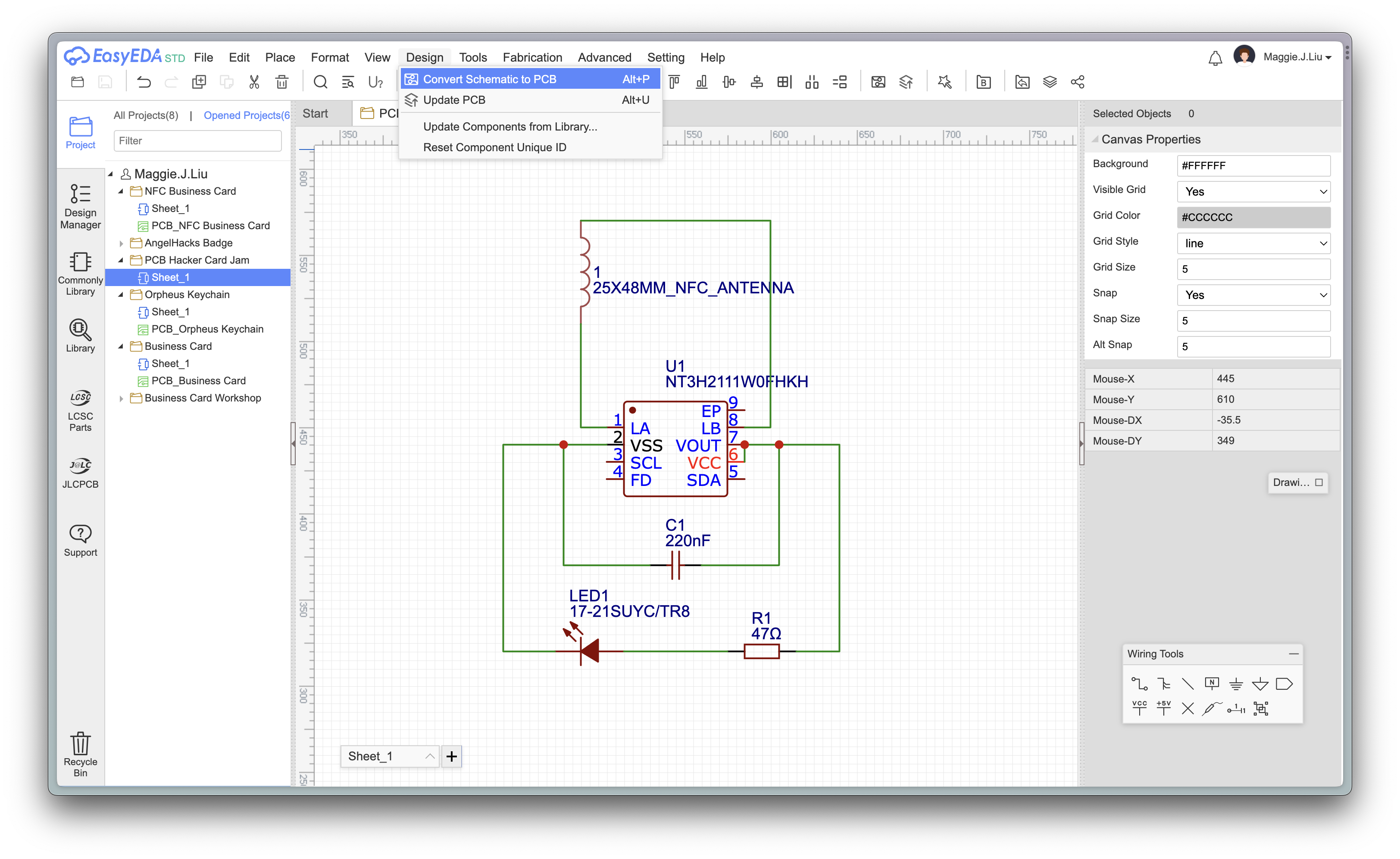
Converting the schematic to a PCB
To convert the schematic into a PCB design file, click Design > Convert Schematic to PCB. You may get a warning about unfinished nets -- this is fine, just click "No, Keep Going."
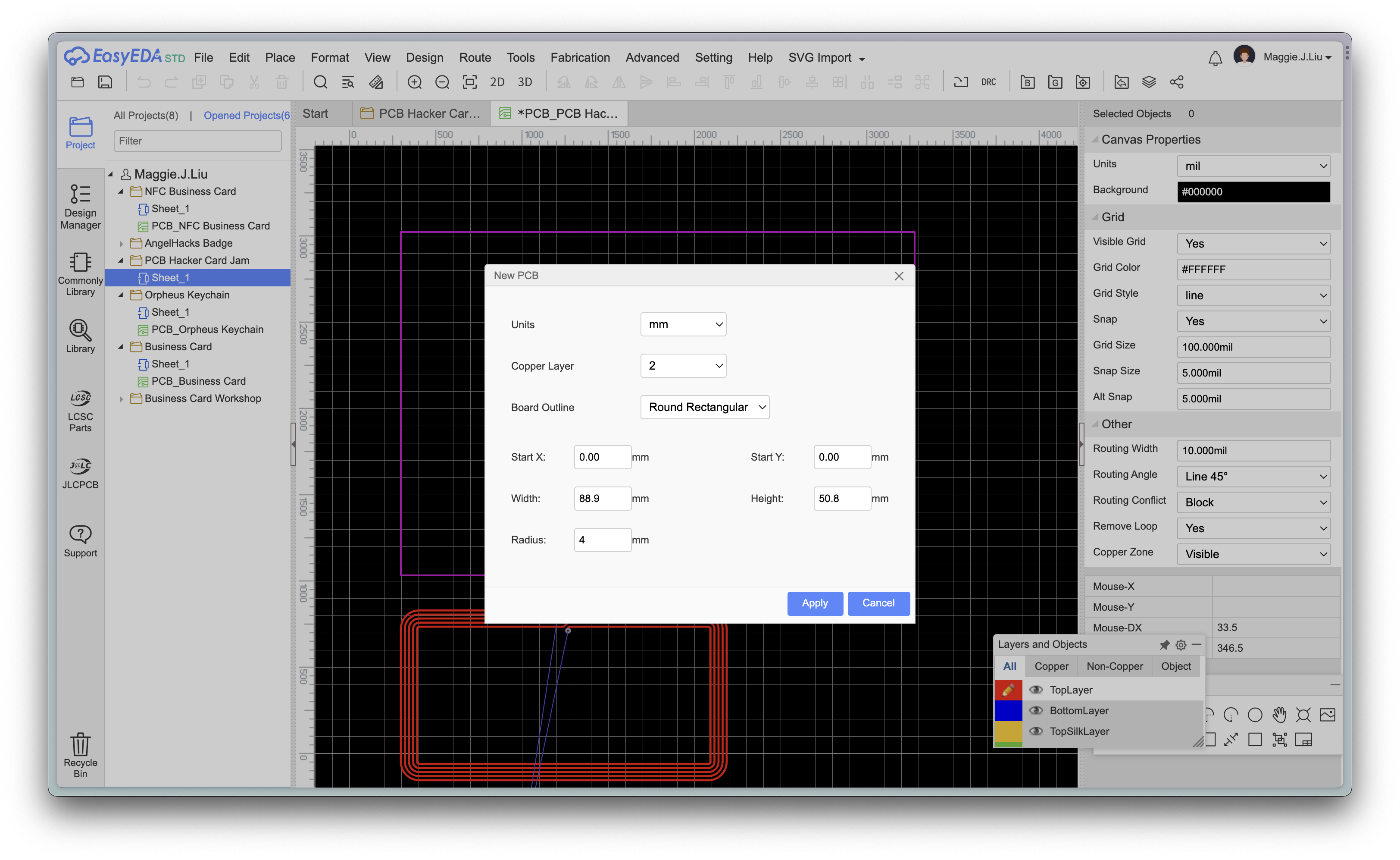
This will open up the PCB editor, as well as a popup window to specify the board's dimensions. (If the popup window doesn't show up for any reason, you can find it through Tools > Set Board Outline.)
Here are the dimensions I'll be using, but feel free to make your business card a different size! Bonus: try making your business card a custom shape (not circular or rectangular). You should have the tools to do that by the end of the jam.
- Board Outline: Round Rectangular
- Width: 88.9mm
- Height: 50.8mm
- Radius: 4mm
Functionality: Making a working PCB card
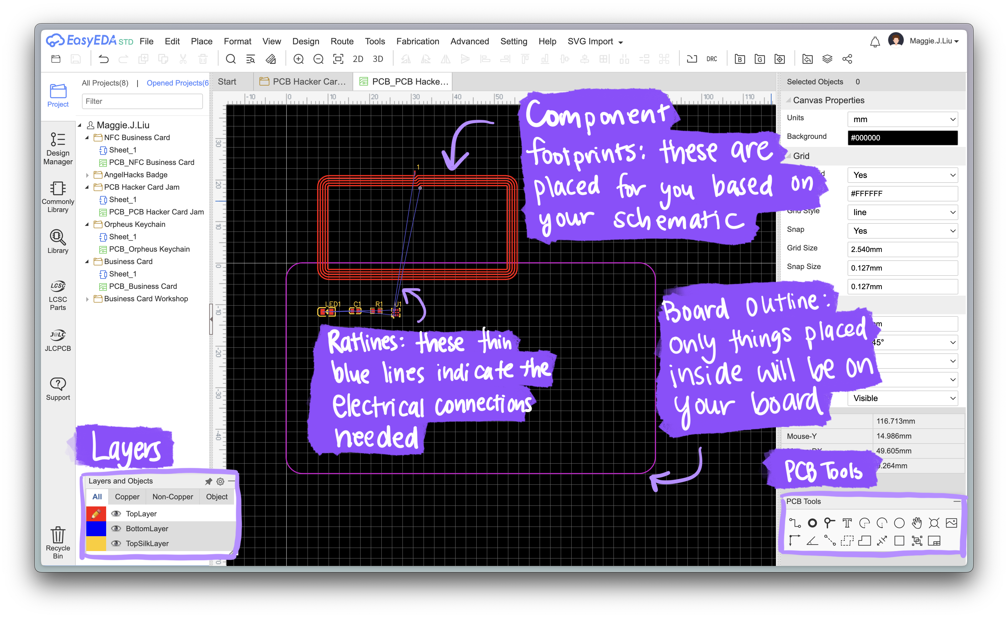
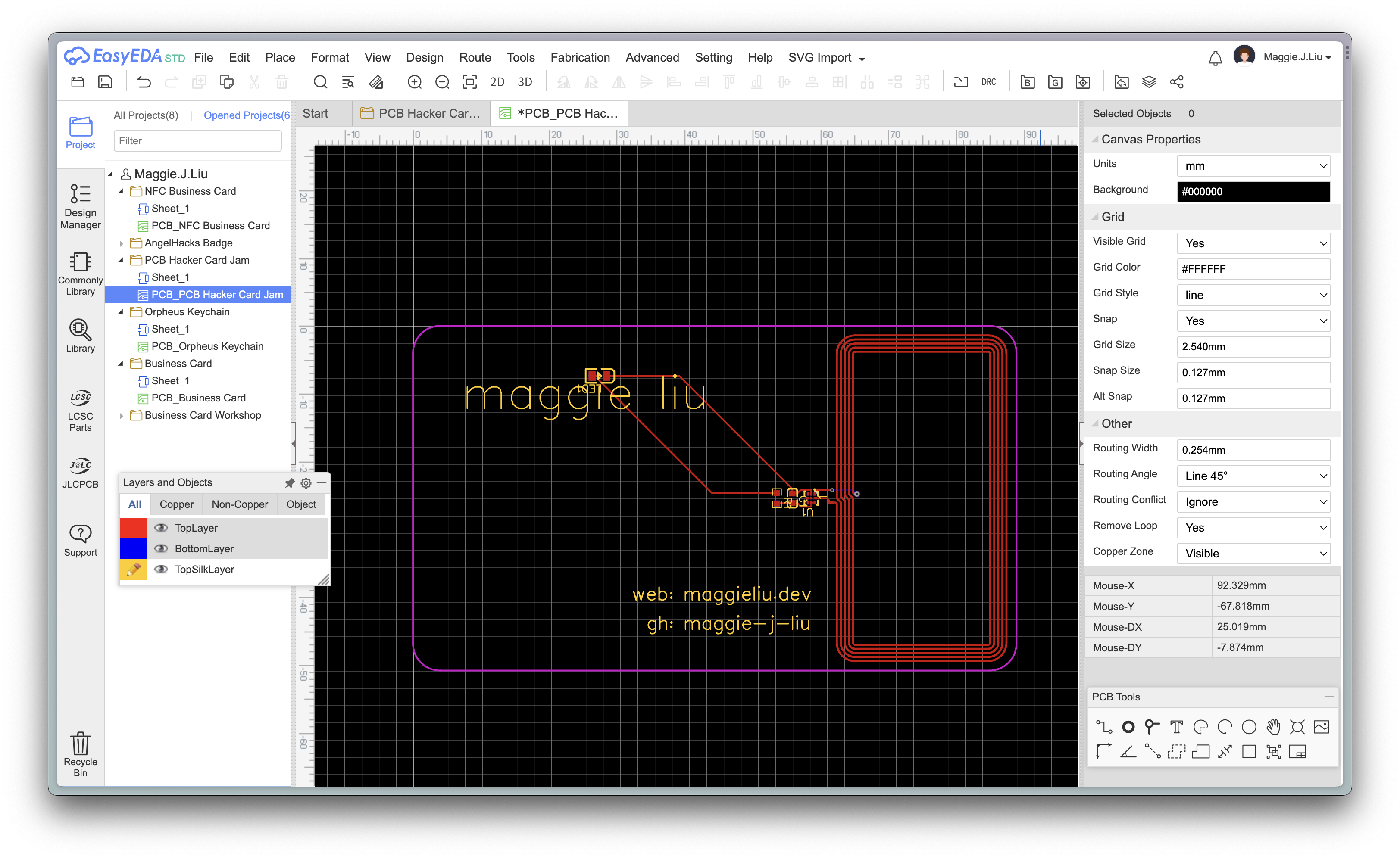
Once you set the board outline, you should see something like the image below. There's the outline of the board in pink, a bunch of components in red, and some thin blue lines connecting the components. Let's talk about what these are, and what the colors mean!
Layers
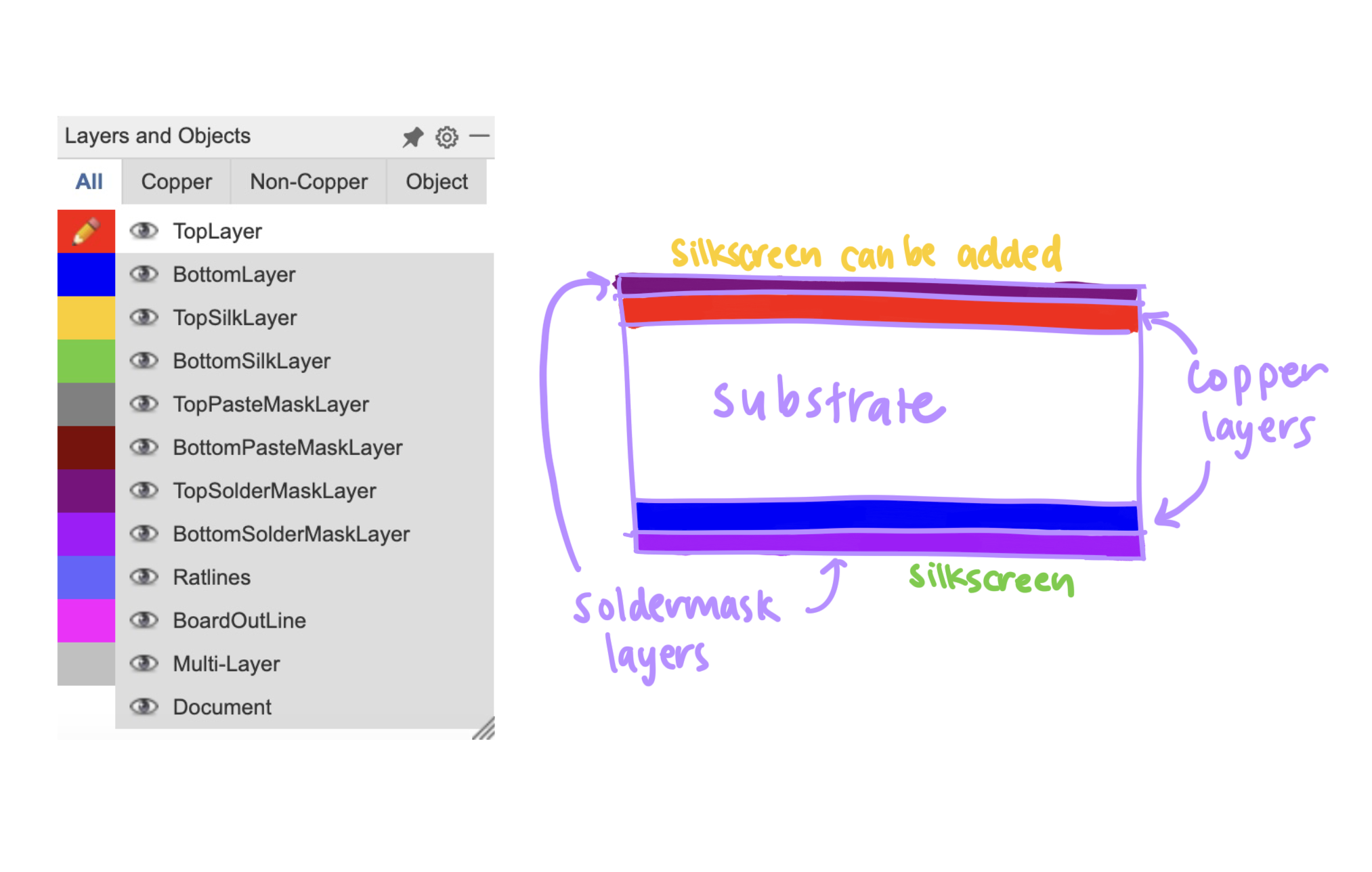
A PCB like a sandwich -- it's made up of many different layers. We're designing a 2-layer PCB, which has the following layers:
- The substrate is in the middle. This makes up the foundation of the PCB, and is usually made of FR-4 (fiberglass).
- On either side of the substrate are copper layers (since this is a 2-layer PCB, there are 2 copper layers: one on top and one on the bottom). In our PCB designer, these are indicated by the
TopLayer(red) andBottomLayer(blue) layers. The copper layers are where electrical connections happen! You should place traces (lines that form electrical connections between components) on theTopLayerandBottomLayer. - On top of the copper layers are soldermask layers. This is what gives PCBs their color -- common soldermask colors are green or black, but white, purple, blue, red, yellow, and more are also possible. Soldermask is added to the entire surface of the board (both the top and the bottom) by default. If you want to remove the soldermask (which will reveal the copper underneath), use the
TopSolderMaskLayerorBottomSolderMaskLayer(for the top and bottom of the board, respectively). - On top of the soldermask layers are silkscreen layers. Silkscreen is usually white, and is generally used to label and identify components, but we'll be using it for ✨ PCB art ✨. We can use this to add contact info, a QR code, or even some illustrations to our business card. In EasyEDA, silkscreen is added on the
TopSilkLayerandBottomSilkLayer.
Components
You'll notice that the PCB designer already has your components populated on the board. By converting the schematic to a PCB design, EasyEDA automatically places the footprints of the components on the board. Try dragging these around! You're able to place them anywhere, but keep in mind that they must be placed within the pink board outline. This is exactly how the components will be placed on the final board.
Some helpful tips:
- You can hit the
Rkey to rotate a component 90 degrees. - The thin blue lines indicate where electrical connections need to be made; so try to rotate components so that the lines do not cross
- Don't worry if the yellow marks cross (that's just silkscreen), but the red parts should not be touching! (That's the copper layer, and if they touch, it will cause a short circuit.)
Drag the components around until you're happy with the placement. Here's what mine looks like, but don't copy it directly; almost anything will work!
Routing traces
Now, we have a bunch of components on the card. If we were to have the card manufactured right now, it wouldn't work -- the components are not connected to each other! We need to add traces to connect the components together.
It's best practice to manually route your traces, using the first button in the PCB tools panel: the Track tool.
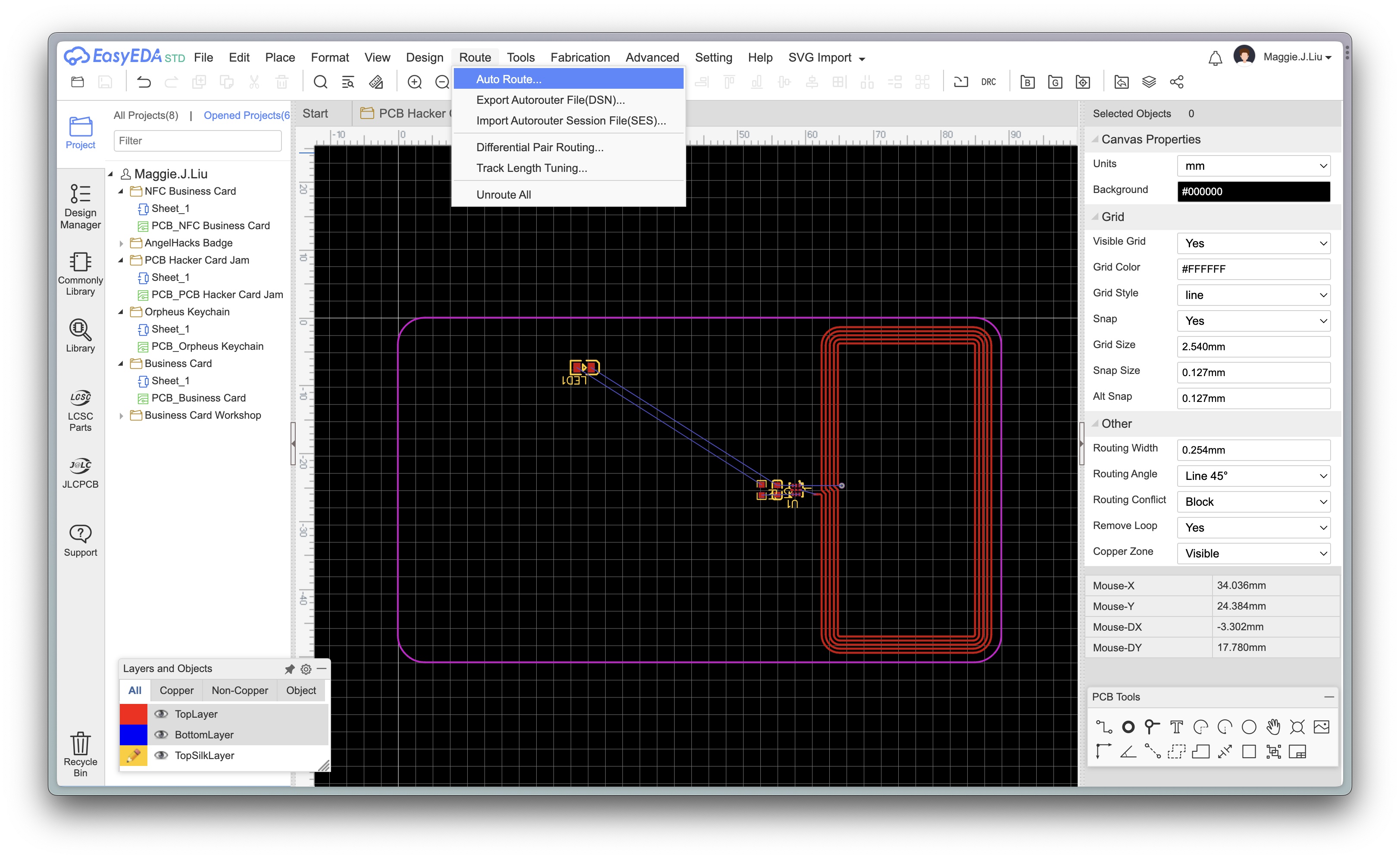
However, to speed up the jam a bit, we'll be using EasyEDA's auto-router. Select Route > Auto Route... and click Run to watch the magic happen...
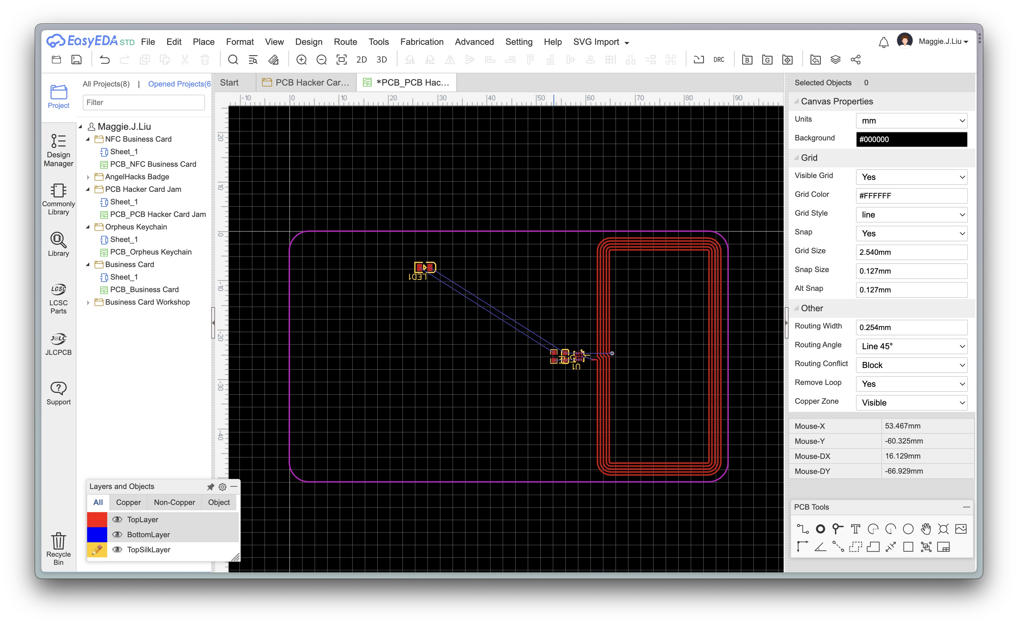
...Except, it seems like the magical autorouter 🪄 wasn't 100% successful :(. We'll finish up the last bit with some manual routing.
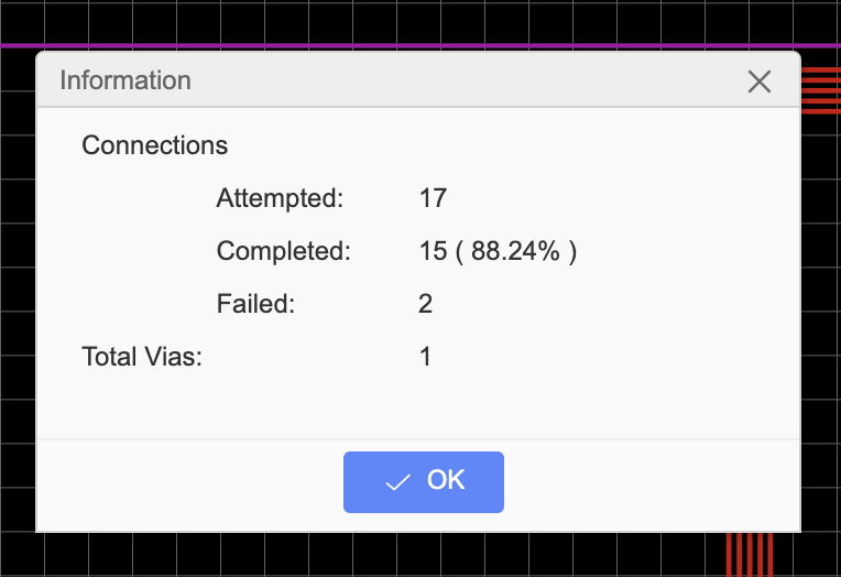
In my case, the autorouter was able to connect most of the components, but there's still one thin blue line (representing an unrouted connection). Can you find it?
Zooooming in, we see that it's between the antenna loop and pin #8 on the NFC chip. Here's how to route it:
- Click the
Tracktool in the PCB Tools panel - On the right sidebar, set
Routing ConflicttoIgnore. This step is generally not needed (for normal manual routing), but there's a small issue with the footprints that makes it necessary here. - Click between the two pads that need to be connected. The thin blue line should disappear, and a red trace should connect the two pads.
Now, your PCB card is functional. Woooo! 🎉
WARNING: Make sure your design has no short circuits
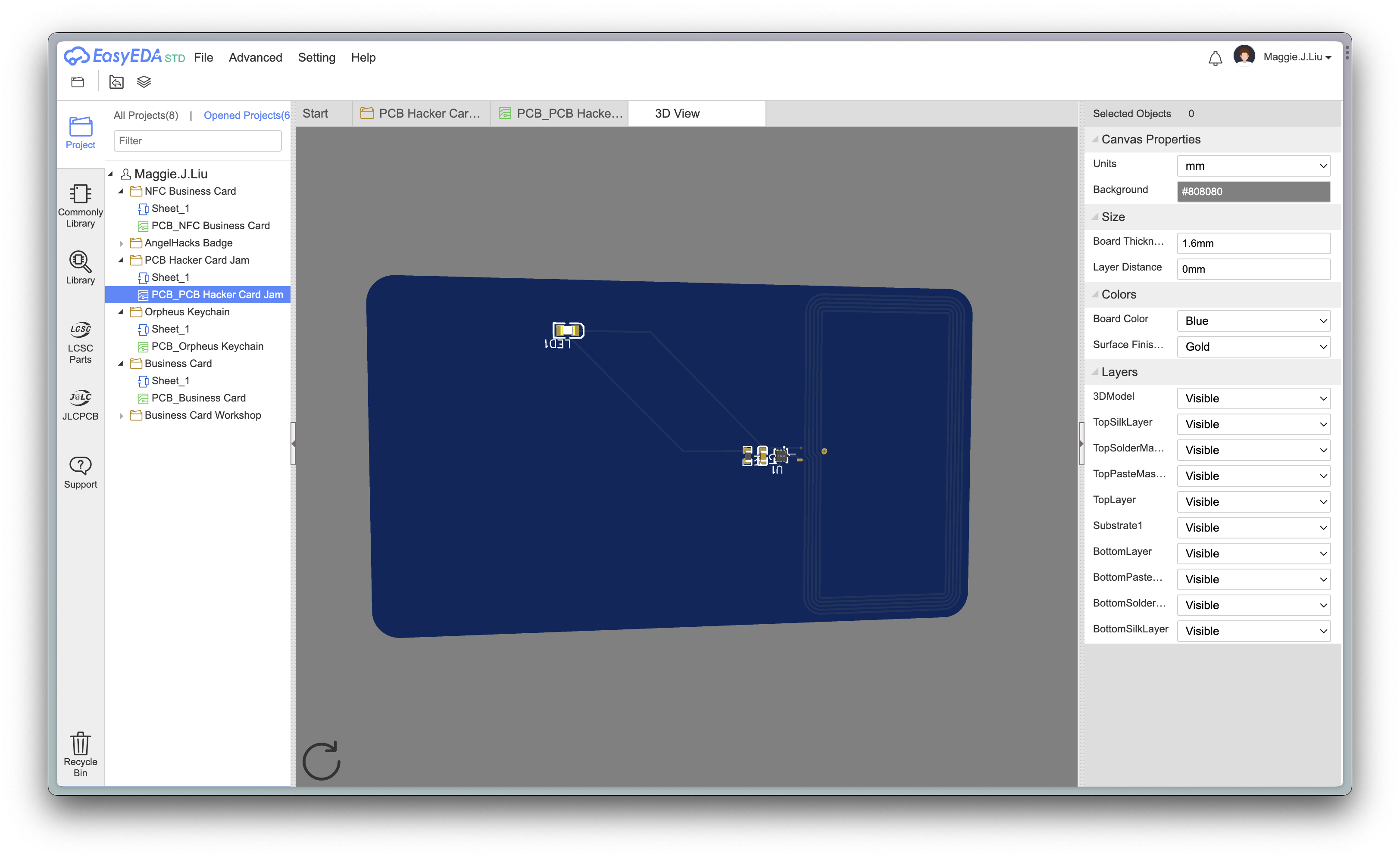
Remember to save your progress! We can check out a preview by clicking the 3D button in the top toolbar. Hmmm... doesn't look like a business card yet. Let's add some personality to it!
Aesthetics: Personalizing your card
We'll mostly be using the silkscreen layer to add our information and designs. Select the TopSilkLayer by clicking the yellow rectangle in the Layers and Objects panel. This will make sure that you're on the silkscreen layer.
Adding text
In the PCB Tools panel, select the Text tool. If you want to make it a business card, you can add your name and contact info -- or add any other text you want. Select the text object you just placed, and change the font, line width, and size in the right sidebar.
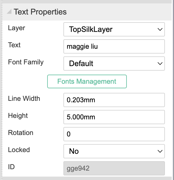
Drag the text to where you want it on your board. Here, I've added my name, website, and GitHub. If you need ideas: you can add your email, phone number, or other social media handles.
Adding a QR Code
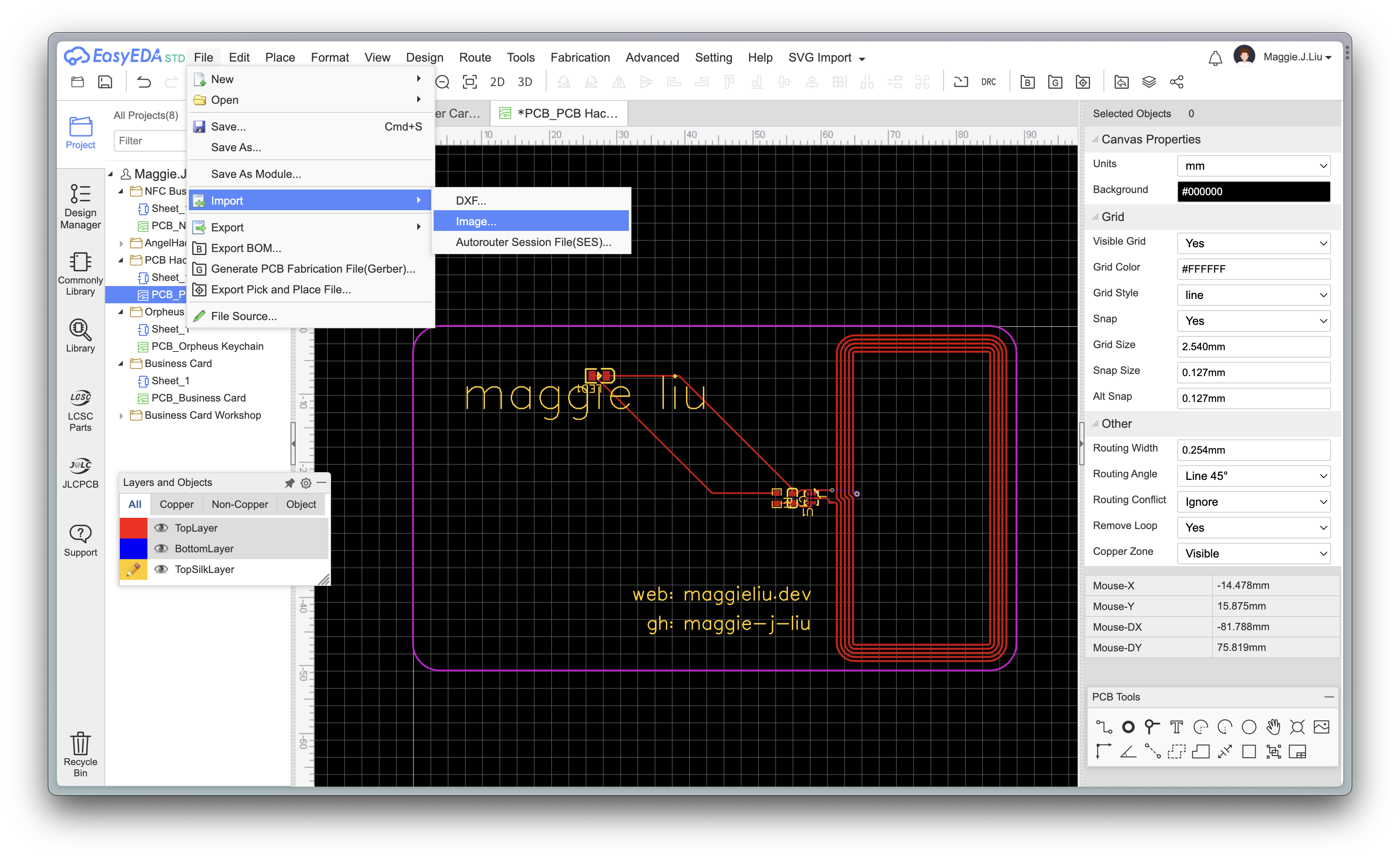
EasyEDA also supports importing images! I'll use this to add a QR Code that links to my website. I used QRCode Monkey to generate a QR Code, then use the File > Import > Image option to import it.
Just like Text objects, you can select the image to modify the properties (width, height, etc.) on the right sidebar.
Note: we've been placing everything on the yellow TopSilkLayer. This means that they will all appear on the top side of our board. If you want to add anything to the bottom, use the green BottomSilkLayer! Keep in mind that the bottom layers of the board are a top-down, see through view, which is essentially flipped -- use the 3D viewer to check that all your text and images are oriented correctly.
Bonus: Textures and other effects
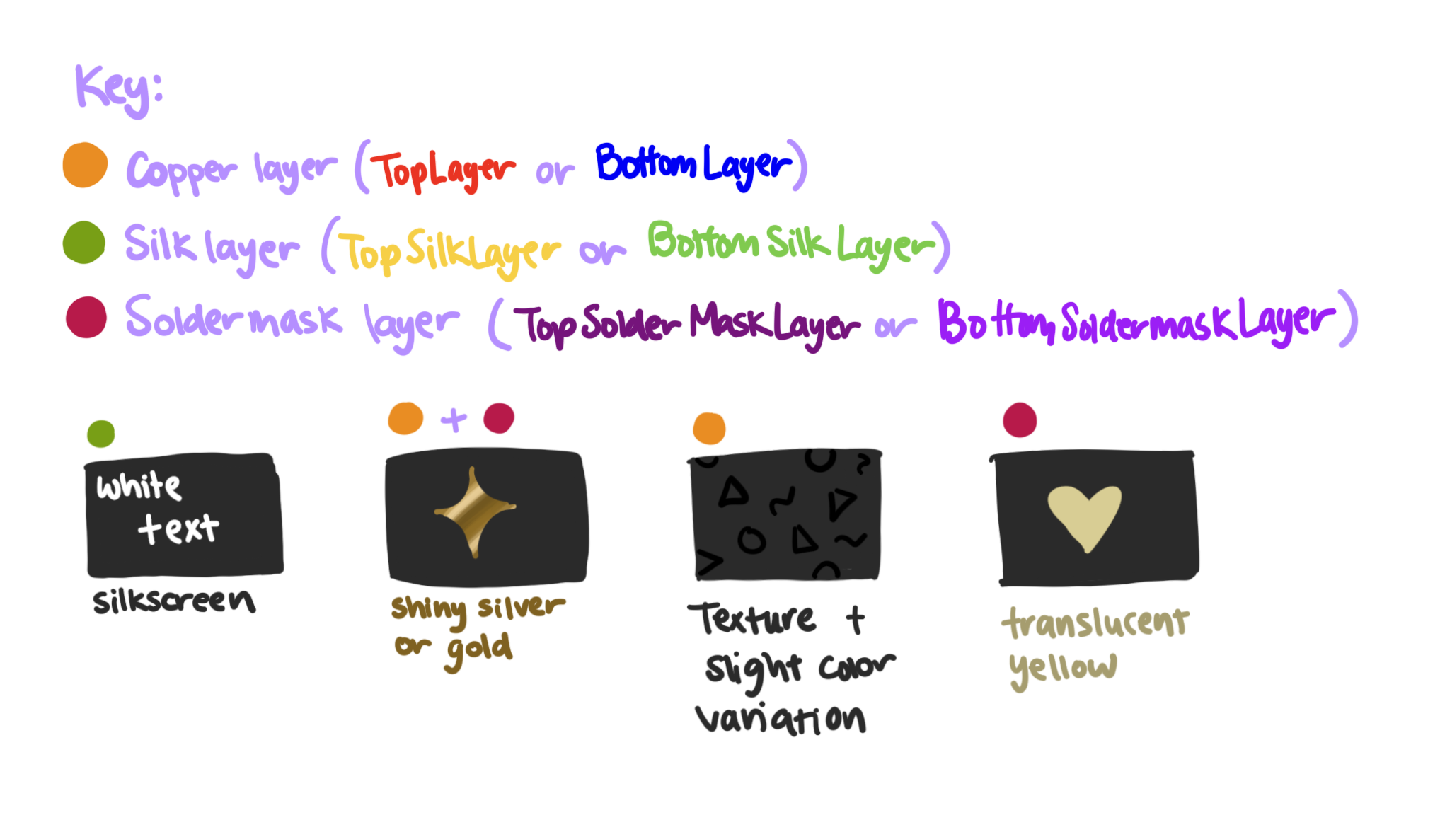
Thus far, we've only used silkscreen to add designs and text to our board. The silkscreen will show up white on the manufactured board, but it's also possible to achieve a variety of other effects by combining different layers!
Here are some examples -- try incorporating these techniques into your board.
- White silkscreen: this is what we've been using. Add things to the
TopSilkLayerorBottomSilkLayerto achieve this effect. - Shiny silver or gold (depends on the finish selected when ordering): add your object to both the
TopLayerandTopSolderMaskLayer(for the top of the board), or to bothBottomLayerandBottomSolderMaskLayer(for the bottom of the board), and superimpose these layers on top of each other. TheTopLayerorBottomLayerwill put the shiny copper on your object, while theTopSolderMaskLayerorBottomSolderMaskLayerwill remove the soldermask on the object, revealing the shiny copper underneath. - Textured, or with slight color variation: add your object to only the
TopLayerorBottomLayer. Without removing the soldermask, the copper will still be covered by the soldermask, but it may slightly lighten the soldermask color and will create a textured feel. - Translucent yellow (color of the FR-4 material): add our object to only the
TopSolderMaskLayerorBottomSolderMaskLayer. This will remove the soldermask on the object, revealing the yellow FR-4 material underneath. This technique is useful for allowing LEDs to shine from one side of the board to the other, or just for adding another color to your design.
Turn your design... into an actual card!
Now that you've got an amazing design, you can actually get your card manufactured and have it in your hands in a few weeks!
Hack Club's OnBoard grant gives high schoolers $100 to manufacture their own PCB designs, and you can use it to get your own card manufactured.
If you're in a club or afterschool group that meets for an hour you're probably reaching the end of your meeting around now. Next meeting you can get started with the OnBoard grant tutorial to order your board for manufacturing.
Congratulations! 🎉 🎉 🎉Share your final project with the community